Recent trends in pcb design
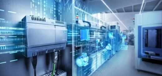
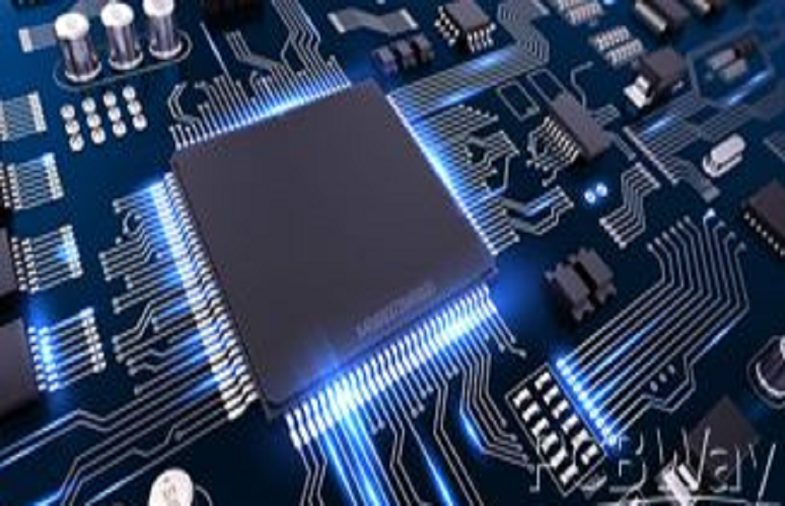
Everything that is operated electronically uses a printed circuit board or PCB. As one of the most significant technological inventions, these tiny electronic circuits are used in many modern devices. Printed circuit boards (PCBs) are required in almost every industry because they are necessary for any product with an electronic component.
Recently, there have been numerous advancements in the PCB manufacturing sector due to how modern technologies like 5G, IoT, and AI have affected the electronics industry. New trends are quickly catching up throughout the PCB creation process. Here are a few fascinating advancements in PCB design.
Board cameras
PCB board cameras have recently undergone a substantial improvement that will increase high-resolution image and video imaging. Board cameras, often called PCB cameras, are tiny cameras directly attached to a PCB and can take pictures. As an illustration, consider medical gadgets like capsule endoscopy units, which may examine your body without invasive surgery.
Although its capture quality and frame rates were initially sacrificed in favor of its compact size, it is already an incredible piece of technology, and makers are constantly looking for methods to improve it. This explains why the megapixel count of smartphone cameras keeps increasing, and the clarity of surveillance film keeps improving. The creation of board cameras will be a significant advancement for both the consumer and industrial electronics markets.
High-density interconnects (HDI)
Unlike conventional PCBs, high-density interconnect (HDI) PCBs offer high-performance and incredibly thin materials. This offers small laser vias, pads, and compact wiring. HDI PCBsare the chosen choice for modern, miniature electronic products. These items utilize reliable PCB prototyping before completing the design.
3-D printed PCBs
The production of PCBs involves several intricate steps. Common PCB design mistakes include erroneous landing patterns, components placed in the wrong orientation, and components placed too close to one another. Making a PCB with a fully functional 3D printer prevents these errors.
Electrical system architecture is changing thanks to 3D printed electronics (3D PEs). 3D PE is an additive manufacturing technique that can create a 3D circuit by printing a substrate layer by layer. Rapid prototyping with quick turnaround is possible thanks to 3D printing. Therefore, there is no prerequisite for a minimum build volume.
With this printing technique, several parts can be produced without requiring assembly. This makes it less likely to create faulty PCBs and enables more complicated PCB design. Due to automation, this will boost overall efficiency and enhance product features.
AR and VR
Tech developments like augmented reality (AR) and virtual reality (VR) are reshaping the consumer electronics industry and influencing PCB design to address difficulties like squeezing electronic packages into odd-shaped packaging. This will validate appropriate circuit operation and lessen the need for place and route techniques. Additionally, since sophisticated simulations can accurately simulate the environment’s magnetic and electric forces, AR using software simulation methods can lower the cost of training operations. This will attest to the product’s compliance with the rules.
Final thoughts
Improvements in PCB design and production methods are becoming more and more necessary because of AI applications. It is essential to reorganize the development cycle to eliminate faults and deliver the product fast.